
-
Products
 Products
 -
Solution
Solution
-
Manufacture
Manufacture
-
Service
Service
-
News
News
-
About us
About us
-
Contact us
Contact us
- Products
- Solution
- Manufacture
- Service
- News
- About us
- Contact us
Fully Automatic Wafer Laser Marking Machine
This equipment is mainly aimed at the etching processing of graphics and logos in semiconductor wafers, and uses the corresponding precise positioning and identification system to realize automatic identification of processed parts Widely used in graphics and logo etching in wafers
- Product description
- Specifications
- Sample display
-
Features:
» This equipment is mainly aimed at the graphics and logo etching processing in semiconductor wafers. It uses the corresponding precise positioning recognition system to realize automatic identification of workpieces. » It uses
multi-axis robots or handling modules to realize the automatic pick-and-place function and complete automatic processing
» Wide application in wafer graphics and logo etching process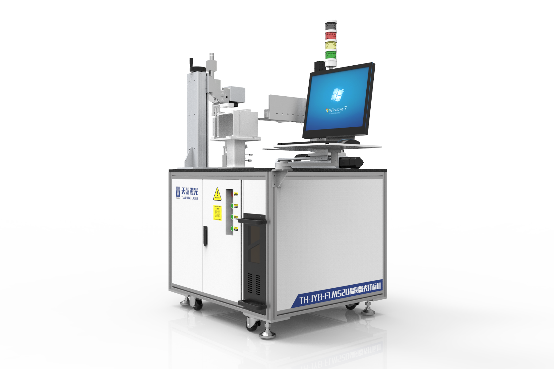
-
Specifications:
-
Sample display:

Wafer marking sample
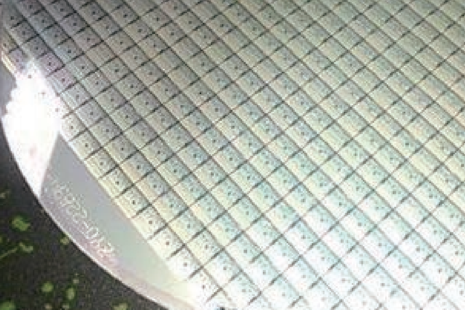 Wafer marking sample
The previous one
Contact us
400-885-0505
Company Address
No. 66, Tonghe Road, Weiting Town, Suzhou Industrial Park
Website
Douyin
